
Geschrieben von Robin
Leitender Ingenieur, Doaho Test (DHT®)
In a laboratory, a tiny semiconductor chip is placed inside a thermal shock chamber. Within minutes, the chamber temperature rapidly rises from -40°C to 125°C, subjecting the chip to extreme thermal expansion and contraction. Under these rapid temperature fluctuations, even minor solder joint cracks or packaging defects are quickly exposed. This is the power of a thermal shock chamber—it allows potential failure risks to be revealed in a controlled, accelerated environment long before the chip reaches the market.
Was ist eine Wärme-Schock-Kammer und wie funktioniert sie?
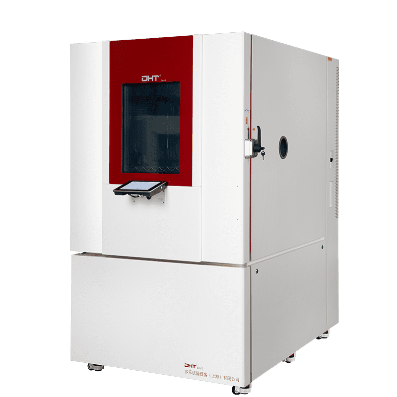
A thermal shock chamber is a specialized testing device designed to rapidly and controllably change the temperature of a test sample. Its core principle lies in the rapid alternation between high and low temperatures, generating intense thermal stress that simulates the extreme conditions a product may encounter during actual use.
Unlike conventional temperature and humidity chambers, thermal shock chambers excel in temperature change rate control. They not only reach the specified high and low temperature extremes but also complete the temperature transition within a very short time. This enables chips, packaging materials, and solder joints to endure sharp thermal gradients in a matter of minutes.
Such thermal shock testing effectively uncovers micro-level defects, such as solder joint stress concentrations, micro-cracks in packaging layers, and material fatigue. By identifying potential failure modes before mass production, engineers gain critical data to optimize design and enhance the reliability of semiconductor chips.
Importance of Thermal Shock Testing for Semiconductor Chips
Semiconductor chips are highly integrated microelectronic devices with complex and delicate internal structures. Temperature fluctuations can cause internal materials to expand or contract unevenly, leading to solder joint fractures, package delamination, or even silicon wafer cracks. This is particularly critical in automotive electronics and aerospace applications, where chips may experience rapid transitions from low-temperature startup to high-temperature operation.
Through thermal shock testing, development teams can replicate these extreme conditions in the laboratory and observe how chips and packaging respond to rapid temperature changes. This not only allows engineers to predict early-life reliability but also provides a scientific foundation for design optimization. For instance, test results may guide engineers to select alternative packaging materials, refine soldering processes, or improve thermal management, significantly reducing failure rates.
Practical Applications and Value of Thermal Shock Chambers
- Assessing Thermal Stress on Elektronikkomponenten: Solder joints and pins are particularly vulnerable to thermal expansion and contraction. Rapid temperature cycling in a thermal shock chamber can reveal fatigue accumulation within hours that would otherwise take weeks or months to manifest. Monitoring electrical parameters and physical damage helps engineers identify weak points early.
- Validating Packaging Material and Structural Reliability: Differences in thermal expansion coefficients among packaging layers can create stress concentrations and micro-cracks. Thermal shock chambers simulate real-world thermal cycles to evaluate the long-term stability of chip packaging structures.
- Testing Chips in Complex Application Environments: Modern chips are widely used in automotive sensors, drone control modules, and industrial automation devices—environments with significant temperature swings. Accelerated thermal shock testing can identify designs prone to failure, providing reliable data to support mass production decisions.
Technical Requirements and Chamber Features
For semiconductor chip testing, the performance of the thermal shock chamber directly impacts the accuracy and reliability of results. High-quality chambers typically feature:
- Rapid Temperature Switching: Quickly alternating between high and low temperatures to generate sufficient thermal stress.
- Temperature Uniformity and Präzision: Ensuring every sample experiences consistent temperature conditions.
- High Reliability and Sicherheit: Long-term, fault-free operation with over-temperature, over-pressure, and fault alarm protections.
- Programmable Test Cycles: Supporting multi-stage temperature profiles and customizable cycles for different chip types and packaging.
- Data Acquisition and Monitoring: Simultaneously recording temperature, electrical parameters, and fault signals to provide comprehensive analysis for engineers.
Practical Value of Thermal Shock Testing in Semiconductor R&D
Thermal shock chambers are more than a testing tool—they are a strategic R&D asset. Through thermal shock testing, companies can:
- Accelerate Product Development: Rapidly simulate extreme temperature fluctuations to uncover solder joint cracks, packaging delamination, or material fatigue, shortening R&D and validation timelines.
- Optimize Packaging and Manufacturing Processes: Use test data to select materials with suitable thermal expansion properties, refine soldering techniques, and enhance heat dissipation design, ensuring chip performance stability.
- Enhance Market Competitiveness: Reliable test data validates product quality, building customer confidence and strengthening brand reputation.
- Reduce Production Risks: Early identification of potential failure modes allows mitigation before mass production, minimizing rework, scrap, and other risks.
Schlussfolgerung
As semiconductor applications become increasingly diverse and market expectations for product reliability rise, thermal shock chambers are indispensable in chip R&D and quality validation. By providing scientific thermal shock testing, development teams can quickly detect design or process vulnerabilities, optimize chip structures and material selection, and ensure stable, durable performance in real-world applications.
For semiconductor products that prioritize high reliability and long service life, thermal shock chambers have become a core laboratory asset.
If you want to make your chip development and testing more efficient and precise, contact DHT® to access professional testing solutions and gain a competitive edge in the market.
Häufig gestellte Fragen
Was ist eine Thermoschockkammer und wie funktioniert sie?
Eine thermische Schockkammer ist ein spezielles Prüfgerät, das eine Probe schnell zwischen hohen und niedrigen Temperaturen wechselt, um intensiven thermischen Stress zu erzeugen. Diese kontrollierte Umgebung simuliert extreme Temperaturbedingungen und hilft Ingenieuren, Mikrodefekte wie Lötstellenrisse, Verpackungsmikrorisse und Materialermüdung vor der Massenproduktion zu erkennen.
Warum ist der Thermoschocktest für Halbleiterchips wichtig?
Halbleiterchips sind hochintegriert und empfindlich gegenüber Temperaturschwankungen. Die thermische Schockprüfung reproduziert schnelle Temperaturänderungen, denen Chips in realen Anwendungen, wie beispielsweise der Automobilelektronik oder der Luft- und Raumfahrt, ausgesetzt sein können. Sie hilft, die Zuverlässigkeit in der frühen Lebensphase vorherzusagen, Verpackungs- und Lötprozesse zu optimieren und die Ausfallraten im Endprodukt zu reduzieren.
What practical benefits does a thermal shock chamber provide in chip F&E?
Thermoschockkammern beschleunigen die Produktentwicklung, indem sie potenzielle Mängel frühzeitig aufdecken, die Optimierung von Verpackungsmaterialien und Wärmemanagement ermöglichen, die Wettbewerbsfähigkeit auf dem Markt durch bestätigte Zuverlässigkeit verbessern und Produktionsrisiken verringern, indem sie Fehlermodi vor der Massenproduktion identifizieren.